FPGA
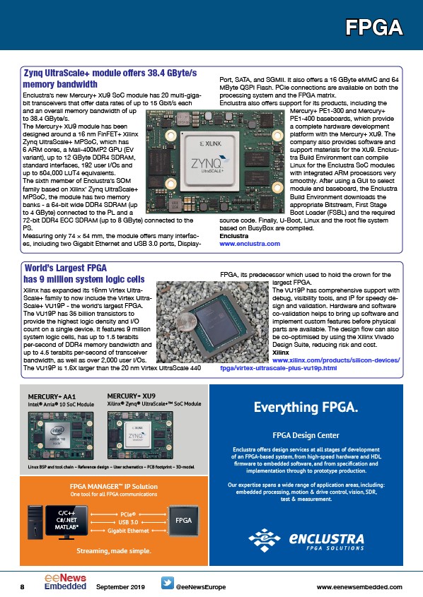
Zynq UltraScale+ module offers 38.4 GByte/s
memory bandwidth
Enclustra’s new Mercury+ XU9 SoC module has 20 multi-gigabit
transceivers that offer data rates of up to 15 Gbit/s each
and an overall memory bandwidth of up
to 38.4 GByte/s.
The Mercury+ XU9 module has been
designed around a 16 nm FinFET+ Xilinx
Zynq UltraScale+ MPSoC, which has
6 ARM cores, a Mali-400MP2 GPU (EV
variant), up to 12 GByte DDR4 SDRAM,
standard interfaces, 192 user I/Os and
up to 504,000 LUT4 equivalents.
The sixth member of Enclustra’s SOM
family based on Xilinx’ Zynq UltraScale+
MPSoC, the module has two memory
banks - a 64-bit wide DDR4 SDRAM (up
to 4 GByte) connected to the PL and a
72-bit DDR4 ECC SDRAM (up to 8 GByte) connected to the
PS.
Measuring only 74 × 54 mm, the module offers many interfaces,
including two Gigabit Ethernet and USB 3.0 ports, Display-
World’s Largest FPGA
has 9 million system logic cells
Xilinx has expanded its 16nm Virtex Ultra-
Scale+ family to now include the Virtex Ultra-
Scale+ VU19P - the world’s largest FPGA.
The VU19P has 35 billion transistors to
provide the highest logic density and I/O
count on a single device. It features 9 million
system logic cells, has up to 1.5 terabits
per-second of DDR4 memory bandwidth and
up to 4.5 terabits per-second of transceiver
bandwidth, as well as over 2,000 user I/Os.
The VU19P is 1.6X larger than the 20 nm Virtex UltraScale 440
Port, SATA, and SGMII. It also offers a 16 GByte eMMC and 64
MByte QSPI Flash. PCIe connections are available on both the
processing system and the FPGA matrix.
Enclustra also offers support for its products, including the
Mercury+ PE1-300 and Mercury+
PE1-400 baseboards, which provide
a complete hardware development
platform with the Mercury+ XU9. The
company also provides software and
support materials for the XU9. Enclustra
Build Environment can compile
Linux for the Enclustra SoC modules
with integrated ARM processors very
smoothly. After using a GUI to select
module and baseboard, the Enclustra
Build Environment downloads the
appropriate Bitstream, First Stage
Boot Loader (FSBL) and the required
source code. Finally, U-Boot, Linux and the root file system
based on BusyBox are compiled.
Enclustra
www.enclustra.com
FPGA, its predecessor which used to hold the crown for the
largest FPGA.
The VU19P has comprehensive support with
debug, visibility tools, and IP for speedy design
and validation. Hardware and software
co-validation helps to bring up software and
implement custom features before physical
parts are available. The design flow can also
be co-optimised by using the Xilinx Vivado
Design Suite, reducing risk and cost.
Xilinx
www.xilinx.com/products/silicon-devices/
fpga/virtex-ultrascale-plus-vu19p.html
MERCURY+ AA1
Intel® Arria® 10 SoC Module
MERCURY+ XU9
Xilinx® Zynq® UltraScale+™ SoC Module
Linux BSP and tool chain – Reference design – User schematics – PCB footprint – 3D-model
FPGA MANAGER™ IP Solution
One tool for all FPGA communications
USB 3.0
USB 3.0
PCle®
USB 3.0
PCIe® Gen3
PCIe® Gen3
Gigabit Ethernet
Gigabit Ethernet
C/C++
C#/.NET
MATLAB®
Gigabit Ethernet
C/C++
C#/.NET
MATLAB®
Streaming, made simple.
FPGA Design Center
Enclustra offers design services at all stages of development
of an FPGA-based system, from high-speed hardware and HDL
firmware to embedded software, and from specification and
implementation through to prototype production.
Our expertise spans a wide range of application areas, including:
embedded processing, motion & drive control, vision, SDR,
test & measurement.
FPGA
FPGA
124.19EC.024 RZ News Inserate AA1 und XU9 190x90.indd 1 04.07.19 13:05
8 Embedded September 2019 @eeNewsEurope
www.eenewsembedded.com
/eenewseurope
/www.enclustra.com
/
/.NET
/.NET
/www.eenewsembedded.com
/www.enclustra.com