NEWS & TECHNOLOGY PHOTONICS
Microlenses self-assembled from liquid crystal deliver 4-D images
UBy Julien Happich sing a self-assembly process, researchers from Nanjing
University have
leveraged the optical
anisotropic properties
of liquid crystals to create
a concentric array of microlenses
able to simultaneously
acquire 3-D space
and polarization information,
hence producing
so-called 4-D images.
Polarized light contains
waves that undulate in
a single plane, whereas
non-polarized light, such
as that from the sun,
contains waves that move
in every direction. Light
can become polarized by
reflecting off objects, and
detecting this type of light can reveal hidden information.
Rather than relying on bulky and expensive equipment, all integrated
4-D imaging at
the lens-level could open
up more possibilities
than today’s industrial
use.
Reporting their findings
in a paper titled
“Self-Assembled Asymmetric
Microlenses for
Four-Dimensional Visual
Imaging” published in the ACS Nano journal, the researchers
used a polarized optical microscope to various image objects
with their new lens, under different directions of linearly polarized
light. The microlenses in the array imaged the object differently,
depending on their distance from the object (depth) and
the direction of polarized light, producing 4-D information.
Although the resolution needs to be further improved, the
authors anticipate such self-assembled liquid crystal microlens
arrays could find applications in medical imaging, communications,
displays or remote sensing.
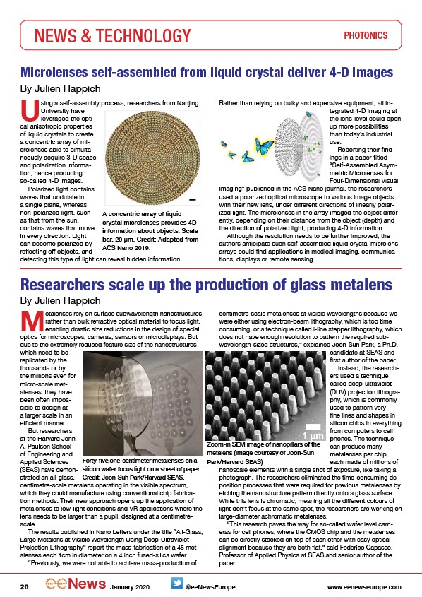
A concentric array of liquid
crystal microlenses provides 4D
information about objects. Scale
bar, 20 μm. Credit: Adapted from
ACS Nano 2019.
Researchers scale up the production of glass metalens
MBy Julien Happich etalenses rely on surface subwavelength nanostructures
rather than bulk refractive optical material to focus light,
enabling drastic size reductions in the design of special
optics for microscopes, cameras, sensors or microdisplays. But
due to the extremely reduced feature size of the nanostructures
which need to be
replicated by the
thousands or by
the millions even for
micro-scale metalenses,
they have
been often impossible
to design at
a larger scale in an
efficient manner.
But researchers
at the Harvard John
A. Paulson School
of Engineering and
Applied Sciences
(SEAS) have demonstrated
an all-glass,
Forty-five one-centimeter metalenses on a
silicon wafer focus light on a sheet of paper.
Credit: Joon-Suh Park/Harvard SEAS.
centimetre-scale metalens operating in the visible spectrum,
which they could manufacture using conventional chip fabrication
methods. Their new approach opens up the application of
metalenses to low-light conditions and VR applications where the
lens needs to be larger than a pupil, designed at a centimetrescale.
The results published in Nano Letters under the title “All-Glass,
Large Metalens at Visible Wavelength Using Deep-Ultraviolet
Projection Lithography” report the mass-fabrication of a 45 metalenses
each 1cm in diameter on a 4 inch fused-silica wafer.
“Previously, we were not able to achieve mass-production of
centimetre-scale metalenses at visible wavelengths because we
were either using electron-beam lithography, which is too time
consuming, or a technique called i-line stepper lithography, which
does not have enough resolution to pattern the required subwavelength
sized structures,” explained Joon-Suh Park, a Ph.D.
candidate at SEAS and
first author of the paper.
Instead, the researchers
used a technique
called deep-ultraviolet
(DUV) projection lithography,
which is commonly
used to pattern very
fine lines and shapes in
silicon chips in everything
from computers to cell
phones. The technique
can produce many
metalenses per chip,
each made of millions of
Zoom-in SEM image of nanopillars of the
metalens (Image courtesy of Joon-Suh
Park/Harvard SEAS)
nanoscale elements with a single shot of exposure, like taking a
photograph. The researchers eliminated the time-consuming deposition
processes that were required for previous metalenses by
etching the nanostructure pattern directly onto a glass surface.
While this lens is chromatic, meaning all the different colours of
light don’t focus at the same spot, the researchers are working on
large-diameter achromatic metalenses.
“This research paves the way for so-called wafer level cameras
for cell phones, where the CMOS chip and the metalenses
can be directly stacked on top of each other with easy optical
alignment because they are both flat,” said Federico Capasso,
Professor of Applied Physics at SEAS and senior author of the
paper.
20 News January 2020 @eeNewsEurope www.eenewseurope.com
/eenewseurope
/www.eenewseurope.com