PHOTONICS
Plasmonics to boost pyroelectric-based hyperspectral sensors
By Julien Happich
Researchers from Duke University have designed frequencytunable
light-trapping plasmonics to speed up the response
of pyroelectric-based sensors, in effect creating a lightweight
and highly
sensitive multispectral
photodetector.
Commercial photodetectors
have already
been designed
with pyroelectric
materials before, but
they haven’t been
able to focus on
specific electromagnetic
frequencies,
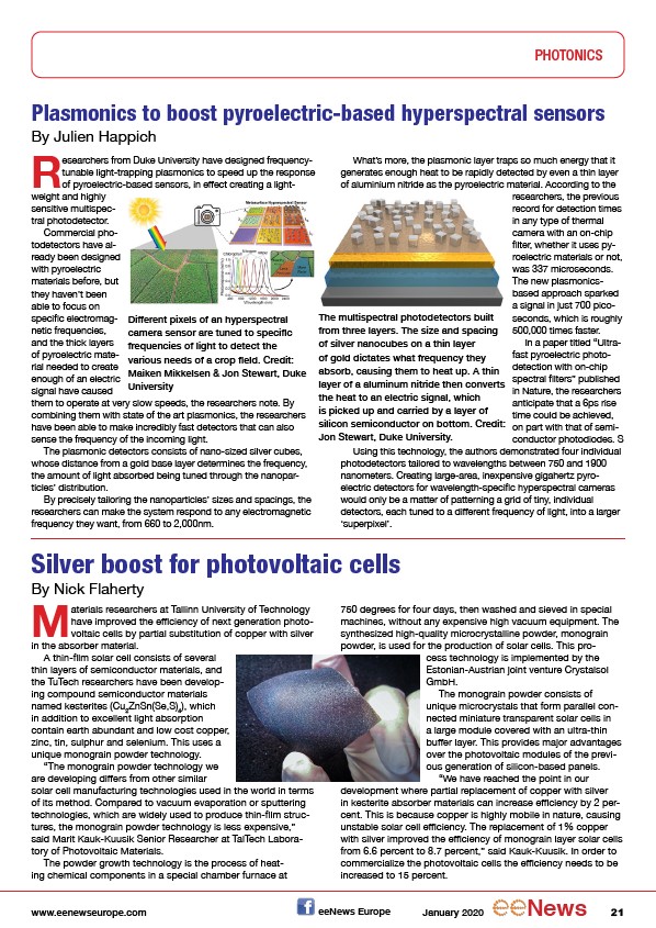
Different pixels of an hyperspectral
camera sensor are tuned to specific
frequencies of light to detect the
various needs of a crop field. Credit:
Maiken Mikkelsen & Jon Stewart, Duke
University
and the thick layers
of pyroelectric material
needed to create
enough of an electric
signal have caused
them to operate at very slow speeds, the researchers note. By
combining them with state of the art plasmonics, the researchers
have been able to make incredibly fast detectors that can also
sense the frequency of the incoming light.
The plasmonic detectors consists of nano-sized silver cubes,
whose distance from a gold base layer determines the frequency,
the amount of light absorbed being tuned through the nanoparticles’
distribution.
By precisely tailoring the nanoparticles’ sizes and spacings, the
researchers can make the system respond to any electromagnetic
frequency they want, from 660 to 2,000nm.
What’s more, the plasmonic layer traps so much energy that it
generates enough heat to be rapidly detected by even a thin layer
of aluminium nitride as the pyroelectric material. According to the
researchers, the previous
record for detection times
in any type of thermal
camera with an on-chip
filter, whether it uses pyroelectric
materials or not,
was 337 microseconds.
The new plasmonicsbased
approach sparked
a signal in just 700 picoseconds,
which is roughly
500,000 times faster.
In a paper titled “Ultrafast
pyroelectric photodetection
with on-chip
spectral filters” published
in Nature, the researchers
anticipate that a 6ps rise
time could be achieved,
on part with that of semiconductor
photodiodes. S
The multispectral photodetectors built
from three layers. The size and spacing
of silver nanocubes on a thin layer
of gold dictates what frequency they
absorb, causing them to heat up. A thin
layer of a aluminum nitride then converts
the heat to an electric signal, which
is picked up and carried by a layer of
silicon semiconductor on bottom. Credit:
Jon Stewart, Duke University.
Using this technology, the authors demonstrated four individual
photodetectors tailored to wavelengths between 750 and 1900
nanometers. Creating large-area, inexpensive gigahertz pyroelectric
detectors for wavelength-specific hyperspectral cameras
would only be a matter of patterning a grid of tiny, individual
detectors, each tuned to a different frequency of light, into a larger
‘superpixel’.
Silver boost for photovoltaic cells
MBy Nick Flaherty aterials researchers at Tallinn University of Technology
have improved the efficiency of next generation photovoltaic
cells by partial substitution of copper with silver
in the absorber material.
A thin-film solar cell consists of several
thin layers of semiconductor materials, and
the TuTech researchers have been developing
compound semiconductor materials
named kesterites (Cu2ZnSn(Se,S)4), which
in addition to excellent light absorption
contain earth abundant and low cost copper,
zinc, tin, sulphur and selenium. This uses a
unique monograin powder technology.
“The monograin powder technology we
are developing differs from other similar
solar cell manufacturing technologies used in the world in terms
of its method. Compared to vacuum evaporation or sputtering
technologies, which are widely used to produce thin-film structures,
the monograin powder technology is less expensive,”
said Marit Kauk-Kuusik Senior Researcher at TalTech Laboratory
of Photovoltaic Materials.
The powder growth technology is the process of heating
chemical components in a special chamber furnace at
750 degrees for four days, then washed and sieved in special
machines, without any expensive high vacuum equipment. The
synthesized high-quality microcrystalline powder, monograin
powder, is used for the production of solar cells. This process
technology is implemented by the
Estonian-Austrian joint venture Crystalsol
GmbH.
The monograin powder consists of
unique microcrystals that form parallel connected
miniature transparent solar cells in
a large module covered with an ultra-thin
buffer layer. This provides major advantages
over the photovoltaic modules of the previous
generation of silicon-based panels.
“We have reached the point in our
development where partial replacement of copper with silver
in kesterite absorber materials can increase efficiency by 2 percent.
This is because copper is highly mobile in nature, causing
unstable solar cell efficiency. The replacement of 1% copper
with silver improved the efficiency of monograin layer solar cells
from 6.6 percent to 8.7 percent,” said Kauk-Kuusik. In order to
commercialize the photovoltaic cells the efficiency needs to be
increased to 15 percent.
www.eenewseurope.com eeNews Europe January 2020 News 21
/
/www.eenewseurope.com