DESIGN & PRODUCTS MEMORY TECHNOLOGIES
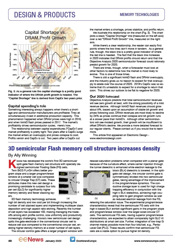
Fig. 3: As a general rule the capital shortage is a pretty good
indicator of where the DRAM profit growth is headed. The
“Capital Shortage” line is derived from CapEx two years prior.
Capital spending’s role
Something interesting always happens when there’s a shortage
and semiconductor manufacturers are profitable: They all
simultaneously invest in additional production capacity. This
phenomenon happened when DRAM prices were high in 2018,
and when NAND flash prices peaked in 2017. The market’s
profitability drives semiconductor cycles. Here’s how.
The relationship between capital expenditures (“CapEx”) and
market profitability is pretty tight: Two years after a CapEx surge
the market enters an oversupply and prices collapse to cost.
Profits vanish and CapEx is cut. Two years after a CapEx cut
the market enters a shortage, prices stabilize, and profits return.
We illustrate this relationship on the chart (Fig. 3). The chart
plots a black “Capital Shortage” line (measured on the left axis)
over a red “DRAM Profit Growth” line, measured on the right
axis.
While there’s a clear relationship, the reader can easily find
points where the two lines don’t move in tandem. As a general
rule, though, the black line is a pretty good indicator of where
the red line is headed. The fact that the black line increases
in 2020 indicates that DRAM profits should return and that the
Objective Analysis 2020 semiconductor forecast could rationally
predict growth for 2020.
There are times, though, when a forecaster must look at
other factors to determine how the market is most likely to
evolve. This is one of those times.
There is still a significant NAND flash and DRAM oversupply,
and the industry gives us no reason to expect for that oversupply
to abate over the course of 2020. 2018’s CapEx was so extreme
that it’s unrealistic to expect for a shortage to return that
soon. This drives our outlook to be flat to negative for 2020.
Our 2020 forecast
Objective Analysis predicts that total semiconductor revenues
will see zero growth at best, with the strong possibility of a mild
revenue decline. Although NAND flash revenues should grow
about 5%, based upon an assumption of stable bit growth and
prices following cost, DRAM revenues are most likely to decline
by 25% as prices continue their collapse and bit growth runs
at a slower pace than NAND’s. Although other semiconductors
will see modest growth, their growth will be insufficient to
offset DRAM’s decline. We provide a more detailed forecast to
our regular clients. Please contact us if you would like to learn
more.
This article first appeared on Electronic Design -
www.electronicdesign.com
3D semicircular Flash memory cell structure increases density
KBy Ally Winning ioxia has developed the world’s first 3D semicircular
split-gate flash memory cell structure with specially designed
semicircular Floating Gate (FG) cells.
Twin BiCS FLASH offers better program
slope and a larger program/erase
window at a smaller cell size compared
to circular Charge Trap (CT) cells. These
attributes make this new cell design a
promising candidate to surpass four bits
per cell (QLC) for significantly higher
memory density and fewer stacking layers.
3D flash memory technology achieves
high bit density and low cost per bit through increasing the
number of cell stacked layers and implementing multilayer stack
deposition and high aspect ratio etching. Recently the number
of cell layers has exceeded 100, making managing the tradeoffs
among etch profile control, size uniformity and productivity
increasingly challenging. Kioxia’s new semicircular cell design
splits the gate electrode in the conventional circular cell to
reduce cell size compared to the conventional circular cell, enabling
higher-density memory at a lower number of cell layers.
The circular control gate offers a larger program window with
relaxed saturation problems when compared with a planar gate
because of the curvature effect, where carrier injection through
the tunnel dielectric is enhanced while electron leakage to the
block (BLK) dielectric is lowered. In the splitgate
cell design, the circular control gate is
symmetrically divided into two semicircular
gates, taking advantage of the improvement
in the program/erase dynamics. The conductive
storage layer is used for high charge
trapping efficiency in conjunction with the
high-k BLK dielectrics, achieving high coupling
ratio to gain program window as well
as reduced electron leakage from the FG,
relieving the saturation issue. The experimental program/erase
characteristics reveal that the semicircular FG cells with the
high-k-based BLK exhibit significant gains in the program slope
and program/erase window over the larger-sized circular CT
cells. The semicircular FG cells, having superior program/erase
characteristics, are expected to attain comparably tight QLC Vt
distributions at small cell size. Further, integration of low-trap Si
channel makes possible more than four bits/cell, e.g., Penta-
Level Cell (PLC). These results confirm that semicircular FG
cells are a viable option to pursue higher bit density.
40 News January 2020 @eeNewsEurope www.eenewseurope.com
/eenewseurope
/www.electronicdesign.com
/www.eenewseurope.com