NEWS & TECHNOLOGY PHOTONICS
Researchers demonstrate silicon-based
particle accelerator
By Julien happich
Researchers at Stanford University have demonstrated the
acceleration of electrons through what they describe as an “Onchip
integrated laser-driven particle accelerator”, detailed in a
recent paper published in the Science journal.
Although the acceleration, demonstrated as an extra 0.915
keV gained along a 30μm-long channel, is only a fraction of
what’s achievable with giant particle accelerators such as the 2
miles long instrument at Stanford’s
SLAC National Accelerator
Laboratory, it is designed
at a scale several orders of
magnitude smaller. Hence,
the researchers anticipate that
hundreds or even thousands of
such silicon-based particle accelerators,
only a few micrometers
in size, could be operated
in cascade to accelerate
particles in useful high-energy
beams.
The researchers carved a
nanoscale channel out of silicon
only 30μm-long, sealed it
in a vacuum and sent electrons
through this cavity while pulses
of infrared light - to which silicon
is transparent - were transmitted
by the channel walls to
speed the electrons along. The
accelerator-on-a-chip demonstrated
in Science is just a
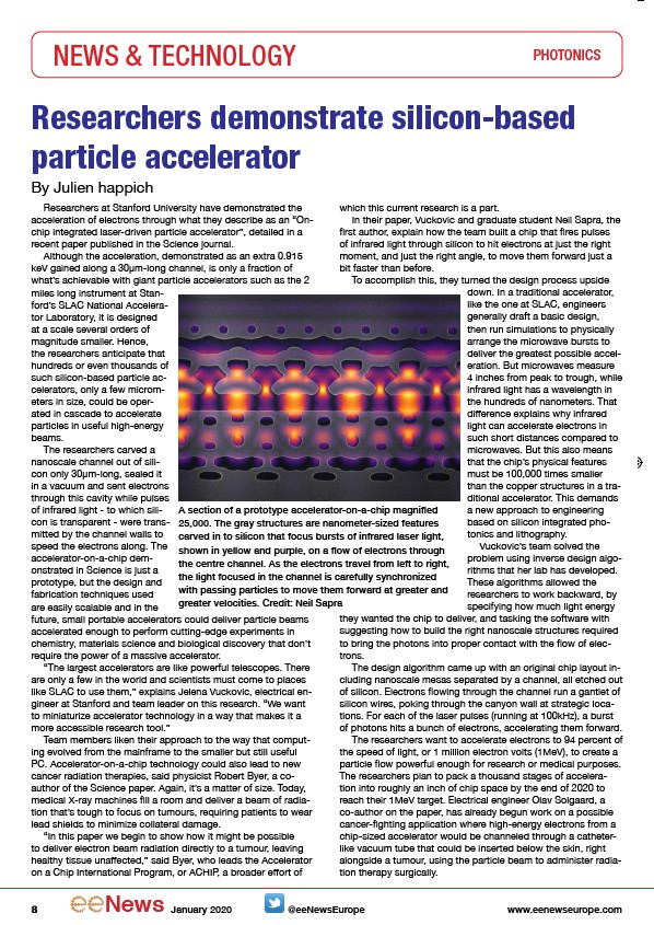
A section of a prototype accelerator-on-a-chip magnified
25,000. The gray structures are nanometer-sized features
carved in to silicon that focus bursts of infrared laser light,
shown in yellow and purple, on a flow of electrons through
the centre channel. As the electrons travel from left to right,
the light focused in the channel is carefully synchronized
with passing particles to move them forward at greater and
greater velocities. Credit: Neil Sapra
prototype, but the design and
fabrication techniques used
are easily scalable and in the
future, small portable accelerators could deliver particle beams
accelerated enough to perform cutting-edge experiments in
chemistry, materials science and biological discovery that don’t
require the power of a massive accelerator.
“The largest accelerators are like powerful telescopes. There
are only a few in the world and scientists must come to places
like SLAC to use them,” explains Jelena Vuckovic, electrical engineer
at Stanford and team leader on this research. “We want
to miniaturize accelerator technology in a way that makes it a
more accessible research tool.”
Team members liken their approach to the way that computing
evolved from the mainframe to the smaller but still useful
PC. Accelerator-on-a-chip technology could also lead to new
cancer radiation therapies, said physicist Robert Byer, a coauthor
of the Science paper. Again, it’s a matter of size. Today,
medical X-ray machines fill a room and deliver a beam of radiation
that’s tough to focus on tumours, requiring patients to wear
lead shields to minimize collateral damage.
“In this paper we begin to show how it might be possible
to deliver electron beam radiation directly to a tumour, leaving
healthy tissue unaffected,” said Byer, who leads the Accelerator
on a Chip International Program, or ACHIP, a broader effort of
which this current research is a part.
In their paper, Vuckovic and graduate student Neil Sapra, the
first author, explain how the team built a chip that fires pulses
of infrared light through silicon to hit electrons at just the right
moment, and just the right angle, to move them forward just a
bit faster than before.
To accomplish this, they turned the design process upside
down. In a traditional accelerator,
like the one at SLAC, engineers
generally draft a basic design,
then run simulations to physically
arrange the microwave bursts to
deliver the greatest possible acceleration.
But microwaves measure
4 inches from peak to trough, while
infrared light has a wavelength in
the hundreds of nanometers. That
difference explains why infrared
light can accelerate electrons in
such short distances compared to
microwaves. But this also means
that the chip’s physical features
must be 100,000 times smaller
than the copper structures in a traditional
accelerator. This demands
a new approach to engineering
based on silicon integrated photonics
and lithography.
Vuckovic’s team solved the
problem using inverse design algorithms
that her lab has developed.
These algorithms allowed the
researchers to work backward, by
specifying how much light energy
they wanted the chip to deliver, and tasking the software with
suggesting how to build the right nanoscale structures required
to bring the photons into proper contact with the flow of electrons.
The design algorithm came up with an original chip layout including
nanoscale mesas separated by a channel, all etched out
of silicon. Electrons flowing through the channel run a gantlet of
silicon wires, poking through the canyon wall at strategic locations.
For each of the laser pulses (running at 100kHz), a burst
of photons hits a bunch of electrons, accelerating them forward.
The researchers want to accelerate electrons to 94 percent of
the speed of light, or 1 million electron volts (1MeV), to create a
particle flow powerful enough for research or medical purposes.
The researchers plan to pack a thousand stages of acceleration
into roughly an inch of chip space by the end of 2020 to
reach their 1MeV target. Electrical engineer Olav Solgaard, a
co-author on the paper, has already begun work on a possible
cancer-fighting application where high-energy electrons from a
chip-sized accelerator would be channeled through a catheterlike
vacuum tube that could be inserted below the skin, right
alongside a tumour, using the particle beam to administer radiation
therapy surgically.
8 News January 2020 @eeNewsEurope www.eenewseurope.com
/eenewseurope
/www.eenewseurope.com