News
ON Semiconductor to buy
Quantenna, targets Wi-Fi
Providing an entry point into the automotive
and industrial low-power connectivity
market, ON Semiconductor Corporation
has entered into a definitive agreement
to acquire Quantenna Communications
for $24.50 per share in an all cash
transaction. The acquisition combines
ON Semiconductor’s expertise in power
management and Bluetooth technologies
with Quantenna’s Wi-Fi and software
capabilities.
“The acquisition of Quantenna is
another step towards strengthening our
presence in industrial and automotive
markets. The combination of ON’s expertise
in highly efficient power management
and broad sales and distribution reach,
and Quantenna’s industry leading Wi-Fi
technologies and software expertise
creates a formidable platform for addressing
fast growing markets for low-power
connectivity in industrial and automotive
applications,” said Keith Jackson, president
and chief executive officer of ON
Semiconductor.
www.onsemi.com
Nestwave demonstrates
low power GPS for IoT
Nestwave, a Paris-based startup, has
developed ultra-low power, advanced
global navigation satellite systems
(GNSS) IP for IoT applications. The IP
was demonstrated at Mobile World
Congress in collaboration with Cadence
by leveraging their Tensilica Fusion F1
DSP platform. When integrated with an
IoT modem such as NB-IoT, Cat M1,
LoRa or Sigfox, the Nestwave low power,
high accuracy GPS IP offers low-cost
geolocation for emerging applications
such as asset tracking, smart factories,
and smart cities, without the need for an
external GNSS chip.
The Cadence Tensilica Fusion F1 DSP
is ideal for low-cost IoT applications
requiring a single processor core that
is proficient at both DSP and controlcode
workloads. Developed on a highly
configurable architecture, the Fusion F1
DSP is specifically designed to excel at
“always-on” processing, including wakeon
voice and sensor fusion applications.
www.nestwave.com
3D printable manufacturing
targets eco-friendly IoT sensors
Simon Fraser University and Swiss
researchers are developing an eco-friendly,
3D printable method
for producing wireless IoT
sensors that can be used and
disposed of without contaminating
the environment. SFU
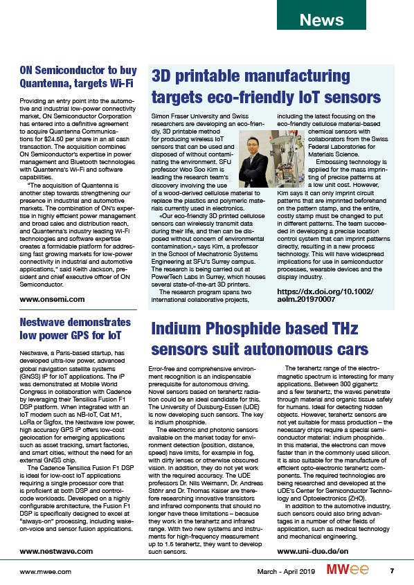
professor Woo Soo Kim is
leading the research team’s
discovery involving the use
of a wood-derived cellulose material to
replace the plastics and polymeric materials
currently used in electronics.
«Our eco-friendly 3D printed cellulose
sensors can wirelessly transmit data
during their life, and then can be disposed
without concern of environmental
contamination,» says Kim, a professor
in the School of Mechatronic Systems
Engineering at SFU’s Surrey campus.
The research is being carried out at
PowerTech Labs in Surrey, which houses
several state-of-the-art 3D printers.
The research program spans two
international collaborative projects,
including the latest focusing on the
eco-friendly cellulose material-based
chemical sensors with
collaborators from the Swiss
Federal Laboratories for
Materials Science.
Embossing technology is
applied for the mass imprinting
of precise patterns at
a low unit cost. However,
Kim says it can only imprint circuit
patterns that are imprinted beforehand
on the pattern stamp, and the entire,
costly stamp must be changed to put
in different patterns. The team succeeded
in developing a precise location
control system that can imprint patterns
directly, resulting in a new process
technology. This will have widespread
implications for use in semiconductor
processes, wearable devices and the
display industry.
https://dx.doi.org/10.1002/
aelm.201970007
Indium Phosphide based THz
sensors suit autonomous cars
Error-free and comprehensive environment
recognition is an indispensable
prerequisite for autonomous driving.
Novel sensors based on terahertz radiation
could be an ideal candidate for this.
The University of Duisburg-Essen (UDE)
is now developing such sensors. The key
is indium phosphide.
The electronic and photonic sensors
available on the market today for environment
detection (position, distance,
speed) have limits, for example in fog,
with dirty lenses or otherwise obscured
vision. In addition, they do not yet work
with the required accuracy. The UDE
professors Dr. Nils Weimann, Dr. Andreas
Stöhr and Dr. Thomas Kaiser are therefore
researching innovative transistors
and infrared components that should no
longer have these limitations – because
they work in the terahertz and infrared
range. With two new systems and instruments
for high-frequency measurement
up to 1.5 terahertz, they want to develop
such sensors.
The terahertz range of the electromagnetic
spectrum is interesting for many
applications. Between 300 gigahertz
and a few terahertz, the waves penetrate
through material and organic tissue safely
for humans. Ideal for detecting hidden
objects. However, terahertz sensors are
not yet suitable for mass production – the
necessary chips require a special semiconductor
material: indium phosphide.
In this material, the electrons can move
faster than in the commonly used silicon.
It is also suitable for the manufacture of
efficient opto-electronic terahertz components.
The required technologies are
being researched and developed at the
UDE’s Center for Semiconductor Technology
and Optoelectronics (ZHO).
In addition to the automotive industry,
such sensors could also bring advantages
in a number of other fields of
application, such as medical technology
and mechanical engineering.
www.uni-due.de/en
www.mwee.com March - April 2019 MW 7
/www.onsemi.com
/www.nestwave.com
/
/en
/www.mwee.com