PROCESSES
Bottom up approach yields atomic-thin FinFETs
By Julien Happich In today’s FinFETs, a semiconducting channel is vertically
wrapped by conformal gate electrodes, and the race is on
to either shrink the fin’s width or move onto gate-all-around
transistors integrating
carbon nanotubes as
the channel. Now a team
of researchers from
the Institute of Metal
Research (IMR) of the
Chinese Academy of
Sciences and CEA Leti
in France has found a
way to further shrink
the fin’s width beyond
what’s achievable with
traditional top-down
fabrication methods.
Indeed, in most
FinFETs, the fin channel
is etched from a bulk
plane, with the width
inherently limited by the
precision of state-of-theart
lithography tools.
As described in a Nature Communication paper titled “A
FinFET with one atomic layer channel”, the researchers have
opted for a bottom-up manufacturing approach to replace the
conventional Si-based fin with an atomic-thin monolayer of a
MoS2, a 2D-material.
To do so, the researchers designed a wet-sprayed chemical
vapor deposition (CVD) method to universally grow monolayers
of transition metal dichalcogenides (ML-TMD) such as MoS2
and WS2 on
step-shaped
templates.
Thanks to this
bottom-up fabrication
approach,
the researchers
were able to
design vertically
free-standing
2D MoS2 and
WS2 monolayers
which they conformally
coated
with insulating
dielectric and
metallic gate
electrodes,
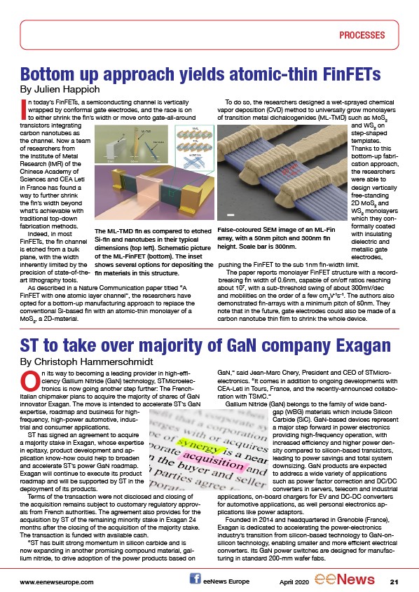
False-coloured SEM image of an ML-Fin
array, with a 50nm pitch and 300nm fin
height. Scale bar is 300nm.
pushing the FinFET to the sub 1nm fin-width limit.
The paper reports monolayer FinFET structure with a recordbreaking
fin width of 0.6nm, capable of on/off ratios reaching
about 107, with a sub-threshold swing of about 300mV/dec
and mobilities on the order of a few cm2V-1s-1. The authors also
demonstrated fin-arrays with a minimum pitch of 50nm. They
note that in the future, gate electrodes could also be made of a
carbon nanotube thin film to shrink the whole device.
The ML-TMD fin as compared to etched
Si-fin and nanotubes in their typical
dimensions (top left). Schematic picture
of the ML-FinFET (bottom). The inset
shows several options for depositing the
fin materials in this structure.
ST to take over majority of GaN company Exagan
By OChristoph Hammerschmidt n its way to becoming a leading provider in high-efficiency
Gallium Nitride (GaN) technology, STMicroelectronics
is now going another step further: The French-
Italian chipmaker plans to acquire the majority of shares of GaN
innovator Exagan. The move is intended to accelerate ST’s GaN
expertise, roadmap and business for highfrequency,
high-power automotive, industrial
and consumer applications.
ST has signed an agreement to acquire
a majority stake in Exagan, whose expertise
in epitaxy, product development and application
know-how could help to broaden
and accelerate ST’s power GaN roadmap.
Exagan will continue to execute its product
roadmap and will be supported by ST in the
deployment of its products.
Terms of the transaction were not disclosed and closing of
the acquisition remains subject to customary regulatory approvals
from French authorities. The agreement also provides for the
acquisition by ST of the remaining minority stake in Exagan 24
months after the closing of the acquisition of the majority stake.
The transaction is funded with available cash.
“ST has built strong momentum in silicon carbide and is
now expanding in another promising compound material, gallium
nitride, to drive adoption of the power products based on
GaN,” said Jean-Marc Chery, President and CEO of STMicroelectronics.
“It comes in addition to ongoing developments with
CEA-Leti in Tours, France, and the recently-announced collaboration
with TSMC.”
Gallium Nitride (GaN) belongs to the family of wide bandgap
(WBG) materials which include Silicon
Carbide (SiC). GaN-based devices represent
a major step forward in power electronics
providing high-frequency operation, with
increased efficiency and higher power density
compared to silicon-based transistors,
leading to power savings and total system
downsizing. GaN products are expected
to address a wide variety of applications
such as power factor correction and DC/DC
converters in servers, telecom and industrial
applications, on-board chargers for EV and DC-DC converters
for automotive applications, as well personal electronics applications
like power adaptors.
Founded in 2014 and headquartered in Grenoble (France),
Exagan is dedicated to accelerating the power-electronics
industry’s transition from silicon-based technology to GaN-onsilicon
technology, enabling smaller and more efficient electrical
converters. Its GaN power switches are designed for manufacturing
in standard 200-mm wafer fabs.
www.eenewseurope.com eeNews Europe April 2020 News 21
/
/www.eenewseurope.com