COVER STORY
directly into the PCB over the lead frame. This new construction
setup leads to a reduction in Rthjc of 22 percent from 1,8 K/W
down to 1,4 K/W.
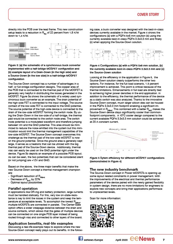
Figure 3: (a) the schematic of a synchronous buck converter
implemented with a half-bridge MOSFET configuration and
(b) example layout of a Drain-Down (in the high side) and
a Source-Down (in the low side) in a half-bridge MOSFET
configuration
The Source-Down concept has a number of advantages in a
half- or full-bridge configuration designs. The copper area of
the PCB that is connected to the thermal pad of the MOSFET is
generally very helpful in distributing the losses generated in the
MOSFET. Figure 3a shows the schematic of a widely used synchronous
buck converter as an example. The drain potential of
the high-side FET is connected to the input voltage. The source
contact of the low-side FET is connected to the GND potential.
The source potential of the high-side device is connected to the
drain of the low-side MOSFET forming the switch node. By using
the Drain-Down in the low-side of a half-bridge, the thermal
pad would be connected to the switch node area. The switch
node potential is a modulated waveform and therefore jumping
between Vin and the GND potential. This area should be minimized
to reduce the noise emitted into the system but this minimization
would limit the thermal management capabilities of the
low-side MOSFET. The Source-Down concept overcomes this
challenge as the thermal pad of the low-side MOSFET is now
on the ground potential. Since the ground area is generally kept
large, it serves as a heatsink that can be utilized with the big
thermal pad of the Source-Down device. Additionally, thermal
vias can easily be used on the GND potential right under the
device. Figure 3b depicts an example of a possible PCB layout.
As can be seen, the two potentials that can be considered silent
(or not jumping) are +12V and GND.
Based on the above, the three major benefits that make the
new Source-Down concept a thermal management champion
are:
- Significant reduction of RDS(on) - Decrease of RthJC by 22%
- Optimal layout possibilities
Parallel operation
In applications like OR-ing and battery protection, large currents
must be handled statically. For this, very low on-state-resistance
is key to limit the losses in the system and keep the temperature
at acceptable levels. To accomplish the lowest RDS(on),
multiple MOSFETs are connected in parallel. The Center-Gate
option offers a wider creepage distance between the drain and
source contacts, which allows that the gates of multiple devices
can be connected on one single PCB layer instead of being
routed through vias and connected to other layers of the board.
Application benefits, real-life examples
Discussing a real-life example helps to explore where the new
Source-Down concept really plays out its benefits. In the following
case, a buck converter was designed with the best-in-class
devices currently available in the market. Figure 4 shows the
configurations (a) with a PQFN 5x6 mm solution (b) using the
currently available best-in-class PQFN 3.3x3.3 mm and finally
(c) when applying the Source-Down solution.
Figure 4 Configurations (a) with a PQFN 5x6 mm solution, (b)
the currently available best-in-class PQFN 3.3x3.3 mm and (c)
the Source-Down solution
Looking at the efficiency in the application in Figure 5, the
Source-Down solution clearly outperforms the other two
options. For instance, for the full load scenario, 1.5 percent
improvement is achieved. This point is critical because of the
thermal limitations. Enhancements in full load are directly tied
to achieving higher power densities in the end application. In
addition to the efficiency, the thermal performance of the device
as a static switch was also analyzed. Thanks to the innovative
Source-Down concept, much larger silicon dies can be housed
in the PQFN 3.3x3.3 mm footprint enabling a significant improvement
in RDS(on). This combined with a better RthJC makes the
Source-Down device stays significantly cooler than commonfootprint
components. A 10°C cooler design compared to the
current available PQFN 3.3x3.3 mm solution could be achieved
at 20 A constant current.
Figure 5 Sytem efficiency for different MOSFET configurations
(demonstrated in Figure 4)
The new industry benchmark
The Source-Down concept in Power MOSFETs is opening up
some layout related constraints in power management. With
the improvements of the electrical and thermal performance
parameters of the device paired with the newly gained flexibility
in system design, there are no more limitations for engineers to
explore new concepts and bring their applications performace
to unprecented levels.
Scan for more information:
www.eenewseurope.com eeNews Europe April 2020 News 7
/
/www.eenewseurope.com