OPTOELECTRONICS
Researchers grow III-V lasers on standard SOI wafers
By RJulien Happich esearchers from the Hong Kong University of Science
and Technology (HKUST) have directly grown 1.5μm III-V
lasers on industry-standard 220nm silicon-on-insulators
(SOI) wafers, without buffer.
Reporting a novel MOCVD growth scheme for the direct
hetero-epitaxy of high-quality III-V alloys on SOI wafers, the
researchers published their findings in the Optica journal under
the title “Bufferless 1.5 μm III-V lasers grown on Si-photonics
220 nm silicon-on-insulator platforms”.
As well as detailing the epitaxy of different dislocation free
III-V compound layers inside trapezoidal troughs on SOI, the
researchers characterized the crystalline quality of these III-V
materials through photoluminescence measurements and
extensive use of transmission electron microscopy.
Based on numerical simulations, they then designed and
fabricated both pure InP and InP/InGaAs air-cladded lasers
on SOI, achieving room-temperature lasing in both the 900nm
band and the 1500nm band under pulsed optical excitation.
Key to efficient light coupling into underlying Si-waveguides,
the new growth scheme eliminates the need for thick
III-V buffers to allow more efficient light coupling into the Siwaveguides.
What’s more, the elimination of the thick buffers
so far needed for III-V lasers on Si can significantly cut down
the growth time and the production cost, the authors write.
Using the new growth scheme, the researchers also claim that
the epitaxial compounds could extend beyond conventional
GaAs and InP and reach highly lattice-mismatched materials
such as GaSb and InAs.
The work by the HKUST researchers could make it possible
to monolithically integrate III-V lasers on industry-standard
220nm SOI wafers in an economical, compact, scalable way.
Next, the researchers want to design and demonstrate the
first electrically driven 1.5μm III-V lasers directly grown on a
220nm SOI platform, and devise a scheme to efficiently couple
light from the III-V lasers into Si-waveguides to conceptually
demonstrate fully integrated Si-photonics circuits.
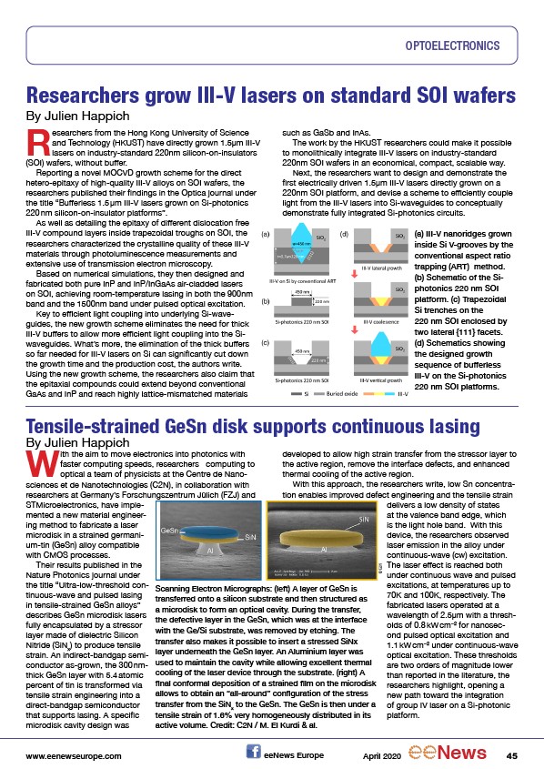
(a) III-V nanoridges grown
inside Si V-grooves by the
conventional aspect ratio
trapping (ART) method.
(b) Schematic of the Siphotonics
220 nm SOI
platform. (c) Trapezoidal
Si trenches on the
220 nm SOI enclosed by
two lateral {111} facets.
(d) Schematics showing
the designed growth
sequence of bufferless
III-V on the Si-photonics
220 nm SOI platforms.
Tensile-strained GeSn disk supports continuous lasing
WBy Julien Happich ith the aim to move electronics into photonics with
faster computing speeds, researchers computing to
optical a team of physicists at the Centre de Nanosciences
et de Nanotechnologies (C2N), in collaboration with
researchers at Germany’s Forschungszentrum Jülich (FZJ) and
STMicroelectronics, have implemented
a new material engineering
method to fabricate a laser
microdisk in a strained germanium
tin (GeSn) alloy compatible
with CMOS processes.
Their results published in the
Nature Photonics journal under
the title “Ultra-low-threshold continuous
wave and pulsed lasing
in tensile-strained GeSn alloys”
describes GeSn microdisk lasers
fully encapsulated by a stressor
layer made of dielectric Silicon
Nitride (SiNx) to produce tensile
strain. An indirect-bandgap semiconductor
as-grown, the 300 nmthick
GeSn layer with 5.4 atomic
percent of tin is transformed via
tensile strain engineering into a
direct-bandgap semiconductor
that supports lasing. A specific
microdisk cavity design was
developed to allow high strain transfer from the stressor layer to
the active region, remove the interface defects, and enhanced
thermal cooling of the active region.
With this approach, the researchers write, low Sn concentration
enables improved defect engineering and the tensile strain
delivers a low density of states
at the valence band edge, which
is the light hole band. With this
device, the researchers observed
laser emission in the alloy under
continuous-wave (cw) excitation.
The laser effect is reached both
under continuous wave and pulsed
excitations, at temperatures up to
70K and 100K, respectively. The
fabricated lasers operated at a
wavelength of 2.5μm with a thresholds
of 0.8 kW cm−2 for nanosecond
pulsed optical excitation and
1.1 kW cm−2 under continuous-wave
optical excitation. These thresholds
are two orders of magnitude lower
than reported in the literature, the
researchers highlight, opening a
new path toward the integration
of group IV laser on a Si-photonic
platform.
Scanning Electron Micrographs: (left) A layer of GeSn is
transferred onto a silicon substrate and then structured as
a microdisk to form an optical cavity. During the transfer,
the defective layer in the GeSn, which was at the interface
with the Ge/Si substrate, was removed by etching. The
transfer also makes it possible to insert a stressed SiNx
layer underneath the GeSn layer. An Aluminium layer was
used to maintain the cavity while allowing excellent thermal
cooling of the laser device through the substrate. (right) A
final conformal deposition of a strained film on the microdisk
allows to obtain an “all-around” configuration of the stress
transfer from the SiNx to the GeSn. The GeSn is then under a
tensile strain of 1.6% very homogeneously distributed in its
active volume. Credit: C2N / M. El Kurdi & al.
www.eenewseurope.com eeNews Europe April 2020 News 45
/
/www.eenewseurope.com