PHOTONICS
Photonic platform delivers
compact beam steering
RBy Julien Happich emoving the need for bulky mechanical
assemblies, researchers
from the Columbia University School
of Engineering and Applied Science are
anticipating that more compact and all-solidstate
LiDARs could be designed based on
a promising new technology, so-called compact
optical phased arrays (OPAs) which they
managed to implement at very low power.
OPAs change the angle of an optical beam
by changing the beam’s phase profile. To
date, long-range, high-performance OPAs
required a large beam emission area densely
packed with thousands of actively phasecontrolled,
power-hungry light-emitting
elements, which made them impractical for
LiDAR applications.
Researchers led by Columbia Engineering
Professor Michal Lipson have developed
a low-power beam steering platform that
is a non-mechanical, robust, and scalable
approach to beam steering. The team is one
of the first to demonstrate low-power largescale
optical phased array at near infrared
and the first to demonstrate optical phased
array technology on-chip at blue wavelength
for autonomous navigation and augmented
reality, respectively.
In collaboration with Adam Kepecs’ group
at Washington University in St. Louis, the
team has also developed an implantable photonic
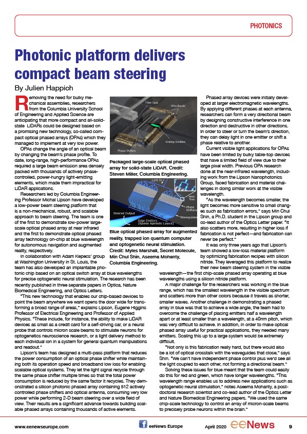
Packaged large-scale optical phased
array for solid-state LiDAR. Credit:
Steven Miller, Columbia Engineering.
Blue optical phased array for augmented
reality, trapped ion quantum computer
and optogenetic neural stimulation.
Credit: Myles Marshall, Secret Molecule,
Min Chul Shin, Aseema Mohanty,
Columbia Engineering.
chip based on an optical switch array at blue wavelengths
for precise optogenetic neural stimulation. The research has been
recently published in three separate papers in Optica, Nature
Biomedical Engineering, and Optics Letters.
“This new technology that enables our chip-based devices to
point the beam anywhere we want opens the door wide for transforming
a broad range of areas,” explains Lipson, Eugene Higgins
Professor of Electrical Engineering and Professor of Applied
Physics. “These include, for instance, the ability to make LiDAR
devices as small as a credit card for a self-driving car, or a neural
probe that controls micron scale beams to stimulate neurons for
optogenetics neuroscience research, or a light delivery method to
each individual ion in a system for general quantum manipulations
and readout.”
Lipson’s team has designed a multi-pass platform that reduces
the power consumption of an optical phase shifter while maintaining
both its operation speed and broadband low loss for enabling
scalable optical systems. They let the light signal recycle through
the same phase shifter multiple times so that the total power
consumption is reduced by the same factor it recycles. They demonstrated
a silicon photonic phased array containing 512 actively
controlled phase shifters and optical antenna, consuming very low
power while performing 2-D beam steering over a wide field of
view. Their results are a significant advance towards building scalable
phased arrays containing thousands of active elements.
Phased array devices were initially developed
at larger electromagnetic wavelengths.
By applying different phases at each antenna,
researchers can form a very directional beam
by designing constructive interference in one
direction and destructive in other directions.
In order to steer or turn the beam’s direction,
they can delay light in one emitter or shift a
phase relative to another.
Current visible light applications for OPAs
have been limited by bulky table-top devices
that have a limited field of view due to their
large pixel width. Previous OPA research
done at the near-infrared wavelength, including
work from the Lipson Nanophotonics
Group, faced fabrication and material challenges
in doing similar work at the visible
wavelength.
“As the wavelength becomes smaller, the
light becomes more sensitive to small changes
such as fabrication errors,” says Min Chul
Shin, a Ph.D. student in the Lipson group and
co-lead author of the Optics Letter paper. “It
also scatters more, resulting in higher loss if
fabrication is not perfect—and fabrication can
never be perfect.”
It was only three years ago that Lipson’s
team showed a low-loss material platform
by optimizing fabrication recipes with silicon
nitride. They leveraged this platform to realize
their new beam steering system in the visible
wavelength—the first chip-scale phased array operating at blue
wavelengths using a silicon nitride platform.
A major challenge for the researchers was working in the blue
range, which has the smallest wavelength in the visible spectrum
and scatters more than other colors because it travels as shorter,
smaller waves. Another challenge in demonstrating a phased
array in blue was that to achieve a wide angle, the team had to
overcome the challenge of placing emitters half a wavelength
apart or at least smaller than a wavelength, at a 40nm pitch, which
was very difficult to achieve. In addition, in order to make optical
phased array useful for practical applications, they needed many
emitters. Scaling this up to a large system would be extremely
difficult.
“Not only is this fabrication really hard, but there would also
be a lot of optical crosstalk with the waveguides that close,” says
Shin. “We can’t have independent phase control plus we’d see all
the light coupled to each other, not forming a directional beam.”
Solving these issues for blue meant that the team could easily
do this for red and green, which have longer wavelengths. “This
wavelength range enables us to address new applications such as
optogenetic neural stimulation,” notes Aseema Mohanty, a postdoctoral
research scientist and co-lead author of the Optics Letter
and Nature Biomedical Engineering papers. “We used the same
chip-scale technology to control an array of micron-scale beams
to precisely probe neurons within the brain.”
www.eenewseurope.com eeNews Europe April 2020 News 9
/
/www.eenewseurope.com